
- Industry-leading 432 GB HBM4 memory capacity with 19.6 TB/s bandwidth enables 400B+ parameter models on a single GPU
- Next-generation TSMC 2nm and 3nm multi-chiplet packaging packing 320 billion transistors
- Open fabric interoperability via UALink, UALoE, and Ultra Ethernet Consortium specifications
- Peak FP4 compute throughput of 40 PFLOPS trails competing next-gen architectures
- Requires ongoing ROCm software stack optimizations to reach operational parity with CUDA
Overview
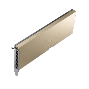
The AMD Instinct MI450 represents a milestone in hyperscale artificial intelligence acceleration, transitioning to AMD’s CDNA 5 architecture built across advanced lithographic nodes. The silicon assembly unites TSMC 2nm compute dies with TSMC 3nm I/O tiles, integrating 320 billion transistors across 12 compute chiplets. The standout architectural achievement is an unprecedented 432 GB HBM4 memory pool delivering 19.6 TB/s of aggregate memory bandwidth, engineered to host large language models exceeding 400 billion parameters entirely within the high-speed local memory footprint of a single accelerator.
From a mechanical and interconnect perspective, the accelerator is designed for enterprise server enclosures utilizing standardized open networking fabrics, including Ultra Accelerator Link (UALink), UALoE, and Ultra Ethernet Consortium (UEC) standards alongside 3.6 TB/s intra-node Infinity Fabric. While comprehensive acoustic and board-level thermal dissipation metrics remain subject to physical teardown and datacenter rack qualification, the immense compute density delivering 40 PFLOPS of FP4 and 20 PFLOPS of FP8 throughput necessitates robust server-chassis airflow and specialized liquid-cooling cold plates.
Operational deployment at scale will be heavily shaped by software stack maturity. Although the hardware specifications establish peerless local memory capacity, enterprise production stability relies on continuous ROCm firmware and driver optimization to achieve software parity with established industry runtimes. For hyperscale AI infrastructure teams, the MI450 offers an open, high-bandwidth compute substrate capable of mitigating multi-node memory latency bottlenecks in frontier AI model training and inference.
Technical Specifications
| Brand | AMD |
| Model | AMD Instinct MI450 |
| Architecture | CDNA 5 |
| Compute Process Node | TSMC 2nm (N2) |
| I/O Process Node | TSMC 3nm (N3P) |
| Transistor Count | 320 billion |
| Chiplet Configuration | 12 compute chiplets |
| Memory Capacity | 432 GB |
| Memory Type | HBM4 |
| Memory Bandwidth | 19.6 TB/s |
| FP4 Compute Throughput | 40 PFLOPS |
| FP8 Compute Throughput | 20 PFLOPS |
| Intra Node Scale Up Bandwidth | 3.6 TB/s |
| Inter Node Scale Out Bandwidth | 300 GB/s |
| Supported Interconnects | Infinity Fabric, UALink, UALoE, UEC |
Primary Sources & Audited Citations
- Oracle First In Line For AMD “Altair” MI450 GPUs, “Helios” Racks
- AMD and Anthropic Announce Strategic Partnership to Deploy Up to 2 Gigawatts of AMD Instinct MI450 Series GPUs
- NVIDIA's next-gen Rubin AI GPUs not delayed, no changes to fight AMD Instinct MI450 AI chips
- Advanced Micro Devices, Inc.: AMD and Anthropic Announce Strategic Partnership to Deploy Up to 2 Gigawatts of AMD Instinct MI450 Series GPUs
- AMD Instinct™ MI400 Series GPUs
- AMD says MI450 GPUs will outperform every Nvidia product including Rubin Ultra
- AMD's Instinct MI450 Reportedly Secures A Major AI Customer
- AMD Instinct MI450 - 2nm, 432 GB HBM4, 40 PFLOPS
- What Is the AMD Instinct MI450? Specs & 2026 Launch
- AMD Instinct MI450X IF128: Rack-Scale AI Explained
- AMD Instinct MI450 GPU Unveiled: CDNA 5 Architecture, 40 PFLOP FP4 ...
- AMD Instinct MI450 Is Coming In 2026 To Challenge NVIDIA ... - HotHardware
- AMD 2.0 - New Sense of Urgency | MI450X Chance to Beat Nvidia ...
- AMD MI400 Series: $7.2B AI GPU Challenging Nvidia [2026]
Recommended Alternatives in Graphics Cards (GPUs)
At a Glance
How reliable is the AMD Instinct MI450 Review: Colossal 432GB memory pushes enterprise compute according to Mizex audits?
An enterprise accelerator with unmatched 432 GB HBM4 memory density for massive model inference, ideal for datacenter operators prioritizing open interconnect standards over proprietary ecosystems.
What are the known quirks or drawbacks of the AMD Instinct MI450 Review: Colossal 432GB memory pushes enterprise compute?
Our reliability audit identified the following documented caveats:
- Peak FP4 compute throughput of 40 PFLOPS trails competing next-gen architectures
- Requires ongoing ROCm software stack optimizations to reach operational parity with CUDA
What are the key engineering highlights of the AMD Instinct MI450 Review: Colossal 432GB memory pushes enterprise compute?
The top strengths recorded in our evaluation include:
- Industry-leading 432 GB HBM4 memory capacity with 19.6 TB/s bandwidth enables 400B+ parameter models on a single GPU
- Next-generation TSMC 2nm and 3nm multi-chiplet packaging packing 320 billion transistors
- Open fabric interoperability via UALink, UALoE, and Ultra Ethernet Consortium specifications